- 您现在的位置:买卖IC网 > Sheet目录530 > UPC8236T6N-E2-A (CEL)IC AMPLIFIER GPS 6-TSON
? PC8236T6N
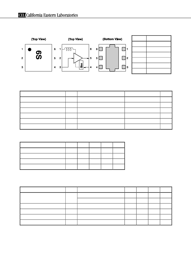
PIN CONNECTIONS AND INTERNAL BLOCK DIAGRAM
Pin No.
1
2
3
4
5
6
Pin Name
V CC
GND
INPUT
Power Save
OUTPUT
V CC
Remark Exposed pad : GND
ABSOLUTE MAXIMUM RATINGS
Parameter
Supply Voltage
Power-Saving Voltage
Total Power Dissipation
Operating Ambient Temperature
Storage Temperature
Input Power
Symbol
V CC
V PS
P tot
T A
T stg
P in
T A = +25 ? C
T A = +25 ? C
Test Conditions
Ratings
4.0
4.0
150
? 40 to +85
? 55 to +150
+10
Unit
V
V
mW
? C
? C
dBm
RECOMMENDED OPERATING RANGE
Parameter
Supply Voltage
Operating Ambient Temperature
Power Save Turn-on Voltage
Power Save Turn-off Voltage
Symbol
V CC
T A
V PSon
V PSoff
MIN.
1.6
? 40
1.0
0
TYP.
2.7
+25
?
?
MAX.
3.3
+85
V CC
0.4
Unit
V
? C
V
V
ELECTRICAL CHARACTERISTICS
(T A = +25 ? C, V CC = V PS = 2.7 V, f in = 1 575 MHz, unless otherwise specified)
Parameter
Circuit Current
Power Gain
Noise Figure
Input Return Loss
Output Return Loss
Symbol
I CC
G P
NF
RL in
RL out
Test Conditions
No Signal (V PS = 2.7 V)
At Power-Saving Mode (V PS = 0 V)
P in = ? 35 dBm
MIN.
5.0
?
17
?
7.5
11
TYP.
6.5
?
19.5
0.8
11
14
MAX.
8.0
1
22
1.1
?
?
Unit
mA
? A
dB
dB ?
dB
dB
2
Data Sheet PU10713EJ01V0DS
发布紧急采购,3分钟左右您将得到回复。
相关PDF资料
UPC8240T6N-E2-A
IC AMPLIFIER GPS 6-TSON
UPD5702TU-EV09
EVAL BOARD UPD5702TU 900MHZ
UPD5713TK-EVAL-A
EVAL BOARD FOR UPD5713TK
UPD5731T6M-E2-A
IC SWITCH SP4T 12-TSQFN
UPD5738T6N-A
IC SWITCH DPDT 6-TSON
UPD5740T6N-E2-A
IC AMPLIFIER GPS 6-TSON
UPG2009TB-EVAL-A
EVAL BOARD FOR UPG2009TB
UPG2010TB-E3-A
IC SWITCH SPDT 6-SMINI
相关代理商/技术参数
UPC8236T6N-EVAL-A
功能描述:GPS开发工具 SiGe LNA IC Eval Board RoHS:否 制造商:STMicroelectronics 产品:Evaluation Boards 工具用于评估:IT600, STM32F20x 频率:1.575 GHz 工作电源电压:1.8 V 接口类型:Wireless
UPC8240T6N-A
功能描述:射频放大器 1575MHz LNA 2.7Volts RoHS:否 制造商:Skyworks Solutions, Inc. 类型:Low Noise Amplifier 工作频率:2.3 GHz to 2.8 GHz P1dB:18.5 dBm 输出截获点:37.5 dBm 功率增益类型:32 dB 噪声系数:0.85 dB 工作电源电压:5 V 电源电流:125 mA 测试频率:2.6 GHz 最大工作温度:+ 85 C 安装风格:SMD/SMT 封装 / 箱体:QFN-16 封装:Reel
UPC8240T6N-E2-A
功能描述:IC AMPLIFIER GPS 6-TSON RoHS:是 类别:RF/IF 和 RFID >> RF 放大器 系列:- 标准包装:3,000 系列:- 频率:100MHz ~ 6GHz P1dB:9.14dBm(8.2mW) 增益:15.7dB 噪音数据:1.3dB RF 型:CDMA,TDMA,PCS 电源电压:2.7 V ~ 5 V 电流 - 电源:60mA 测试频率:2GHz 封装/外壳:0505(1412 公制) 包装:带卷 (TR)
UPC8240T6N-EVAL-A
制造商:California Eastern Laboratories (CEL) 功能描述:SIGE LNA IC EVAL BOARD, ROHS COMPLIANT - Boxed Product (Development Kits) 制造商:California Eastern Laboratories (CEL) 功能描述:EVAL BOARD UPC8240T6N
UPC8244T6N-A
功能描述:IC AMPLIFIER GPS 6-TSON RoHS:是 类别:RF/IF 和 RFID >> RF 放大器 系列:- 标准包装:3,000 系列:- 频率:100MHz ~ 6GHz P1dB:9.14dBm(8.2mW) 增益:15.7dB 噪音数据:1.3dB RF 型:CDMA,TDMA,PCS 电源电压:2.7 V ~ 5 V 电流 - 电源:60mA 测试频率:2GHz 封装/外壳:0505(1412 公制) 包装:带卷 (TR)
UPC8244T6N-E2-A
功能描述:IC AMPLIFIER GPS 6-TSON RoHS:是 类别:RF/IF 和 RFID >> RF 放大器 系列:- 标准包装:3,000 系列:- 频率:100MHz ~ 6GHz P1dB:9.14dBm(8.2mW) 增益:15.7dB 噪音数据:1.3dB RF 型:CDMA,TDMA,PCS 电源电压:2.7 V ~ 5 V 电流 - 电源:60mA 测试频率:2GHz 封装/外壳:0505(1412 公制) 包装:带卷 (TR)
UPC8244T6N-EVAL-A
制造商:California Eastern Laboratories (CEL) 功能描述:SIGE LNA IC EVAL BOARD, ROHS COMPLIANT - Boxed Product (Development Kits) 制造商:California Eastern Laboratories (CEL) 功能描述:EVAL BOARD UPC8244T6N
UPC824C-A
制造商:Renesas Electronics Corporation 功能描述:SEMICONDUCTOR, IC, OP AMP, VOLTAGE, FEED
